If we imagine a perfect amplifier, it should have infinite gain, infinite input impedance, zero output impedance and infinite bandwidth, but in real life, nothing is ideal, so they have limited gain and limited bandwidth.
The term operational amplifier was originally used for DC amplifiers that perform mathematical operations (such as summation, subtraction, integration and differentiation) in analog computers. Operational amplifiers have a much wider range. In addition to amplification, they can also be used in other occasions, such as voltage regulators in instrumentation and control systems.
Operational amplifiers can amplify signals with frequencies ranging from 0 Hz to 1 MHz. This means that op-amp can be used to amplify DC signals (0 Hz) and AC input signals (high frequency signals). In addition, it is designed to connect external components (such as resistors, capacitors, etc.) to its terminals. By adding these passive components, their external characteristics can be changed.
2、 Understand operational amplifier parameters
When designing products, it is essential to understand the characteristics of operational amplifiers, that is, if you want to design products efficiently and minimize costs, you should understand the following parameters of Operational Amplifiers:
2.1. Open loop voltage gain: the most important function of the amplifier is to amplify the signal. Each amplifier has a certain gain, which means that if an input voltage is applied, it will be multiplied by the gain. For example, if the gain of the operational amplifier is 2 * 10 ^ 5 and the input is 2 V, the output voltage is 400000v, which is practically impossible because it means that the operational amplifier is saturated and the output voltage is limited to VCC.
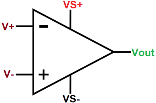
2.2. Input resistance: it is the resistance between the in-phase and inverting inputs of the amplifier.
2.3. Output resistance: the output resistance is just like the internal resistance of the battery, so it is a very small resistance, which means that the output voltage depends on the load.
2.4. Input offset voltage: if we apply the same input voltage to the two terminals of the operational amplifier, the output should be zero volts. In fact, this is impossible because the internal transistors do not have the same value, so a very small voltage will appear at the output terminal. Therefore, to make the output zero, we must apply a small differential voltage, which is called the input offset voltage.
2.5. Input offset current: if we ground both the in-phase and inverting terminals of the operational amplifier, we can see that a small current will flow through the output pin of the operational amplifier. This is the generated current. Because the base current of the internal transistor is different, in order to make the output current zero, a small input current can be applied to offset the output current, which is called the input offset current.
2.6. Input bias current: the input bias current is the average of the currents flowing into the inverting and in-phase input terminals of the operational amplifier. The smaller the input bias current, the smaller the drift.
2.7. CMRR: common mode rejection ratio (CMRR) is defined as the ratio of differential voltage gain to common mode voltage gain. The ability of the differential amplifier to suppress the common mode signal is expressed by the common mode rejection ratio.
2.8. Slope: defined as the maximum change rate of output voltage per unit time, expressed in volts / microsecond. Slew rate indicates the speed at which the output of op-amp can change in response to the change of input frequency 9. Voltage swing: defined as the proximity of output voltage to power supply voltage or the driving degree of output to rail.
2.10. Gain bandwidth product: we know that the voltage gain of the operational amplifier will drop at high frequency due to storage caused by parasitic junction capacitance and minority carrier changes in the device. As the frequency input signal increases, the open-loop gain decreases until it finally reacts to the value of 1. The frequency at which the gain is reduced to 1 is defined as the unit gain frequency or the unit gain bandwidth.
2.11. Peak to peak input noise voltage: if we look at a noise signal, it will have a maximum value point and a minimum value point. The difference between the minimum value and the maximum value is called the peak to peak input noise voltage.
2.12. Unity gain: a unity gain amplifier is an amplifier with a gain of 1, which also means that there is no gain. The output voltage will be the same as the input voltage and is commonly referred to as a voltage follower amplifier.

 Service mailbox
 13823783658
 ChatNow