Among all device characteristics, noise may be a particularly challenging and difficult design topic. This paper mainly introduces the influence of power supply noise on the phase noise of high-speed DAC.
DAC phase noise source
For high-speed DAC, phase noise mainly comes from the following aspects: clock noise, power supply noise, internal noise and interface noise.
Figure 1: DAC phase noise source (picture source: ADI)
The two most important sources are clock noise and power supply noise. This paper will mainly introduce the influence of power supply noise on DAC phase noise.
Phase noise propagation path of DAC power supply
All circuits on the chip must be powered in some way, which provides many opportunities for noise to propagate to the output. The propagation paths of power supply noise in different circuits are also different. Several common DAC power supply noise propagation paths are highlighted below.
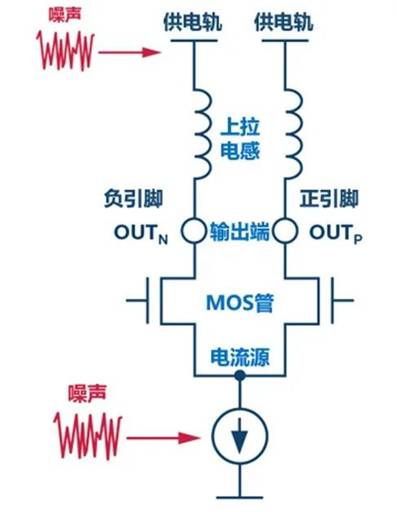
As shown in the figure below, the DAC output terminal is usually composed of a current source and a MOS tube, which guides the current to supply power through the positive pin or the negative pin. The current source obtains power from an external power source, and any noise will be reflected as current fluctuation.
Figure 2: source of DAC power supply noise (picture source: ADI)
MOS tube
The noise of the current source can reach the output through the MOS tube, but this only explains the coupling phenomenon of the noise.
Figure 3: DAC power supply noise propagation path - MOS tube (picture from ADI)
To "contribute" the phase noise, this noise needs to be mixed to the carrier frequency by MOS transistor. The MOS transistor here is equivalent to a balanced mixer.
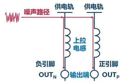
Pull up inductance
The pull-up inductance is another noise path, and the noise flows from the supply rail to the output.
Figure 4: DAC power supply noise propagation path - pull-up inductance (picture source: ADI)
Any change of power supply rail and load will cause current change, thus mixing noise to carrier frequency again.
More noise conduction paths
Generally speaking, if the switching can mix the noise to the carrier frequency, these switching circuits are all contributors to the phase noise of the power supply.
Analyze phase noise
For the above-mentioned mixing phenomenon, it is quite difficult to quickly simulate all these behaviors and improve them. On the contrary, by measuring the power supply rejection ratio, we can quickly understand which power supplies are sensitive to noise, and then select some power supplies with high accuracy and low noise, so as to achieve twice the result with half the effort.
Other analog modules also have similar analysis of power supply rejection ratio, such as voltage regulators, operational amplifiers and other ICs. Generally, power supply rejection ratio is specified.
The power supply suppression performance measures the sensitivity of the load to the power supply change and can be used for the phase noise analysis here. However, the suppression ratio is not used here, but the modulation ratio: power supply modulation ratio (psmr). Of course, the traditional power supply rejection ratio (psmr) still has reference significance.
We specially modulate a noise to test. The next step is to obtain specific data.
Measure psmr
A very important method to analyze phase noise is to measure psmr.
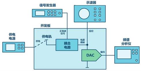
Schematic diagram of typical measurement psmr test:
Figure 5: psmr measurement (picture source: ADI)
Psmr measurement can be divided into three steps: modulating power rail, acquiring data and analyzing data.
Modulated power rail
The power modulation is obtained by a coupling circuit inserted between the power supply and the load, and a sine wave signal generated by the signal generator is superimposed.
get data
The output of the coupling circuit is monitored by an oscilloscope to monitor the actual power modulation. The final DAC output is detected by the spectrum analyzer.
Analysis data
Psmr is equal to the ratio of the AC component of the power supply displayed from the oscilloscope to the modulated sideband voltage around the carrier.
The following are the key points of psmr measurement:
Coupling circuit: there are many different coupling mechanisms in the coupling circuit. The coupling circuit can choose LC circuit, power operational amplifier, transformer or special modulation power supply. The method used here is a 1:100 turn ratio current detection transformer and a function generator. It is recommended to use a high turn ratio to reduce the source impedance of the signal generator.
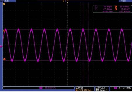
Power modulation: 1.2V DC power is modulated by superimposing a 500KHz peak to peak voltage 38 MV signal.
Figure 6: clock power modulation (picture source: ADI)
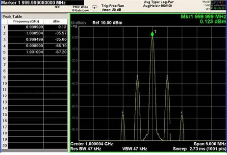
DAC: ad9164 of ADI is adopted. The DAC clock speed is 5gsps. The resulting output causes sidebands on a full-scale 1GHz, – 35dbm carrier.
Figure 7: modulation sideband (picture source: ADI)
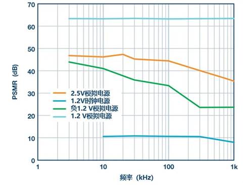
The power is converted into voltage, and then the ratio is calculated by modulating the power supply voltage. The psmr is – 11 dB. The ad9164 has eight power supplies. We choose the key. The key is to scan the following four power supplies: 1.2V clock power supply, negative 1.2V and 2.5V analog power supply, and 1.2V analog power supply. The results are shown in the following figure:
Figure 8: power supply psmr measured by scanning frequency (picture source: ADI)
Clock power supply is the most sensitive power supply rail, followed by negative 1.2V and 2.5V analog power supply, while 1.2V analog power supply is not very sensitive. With proper consideration, the 1.2V analog power supply can be powered by the switching regulator, but the clock power supply is completely opposite: it needs to be powered by the ultra-low noise LDO to obtain high-quality performance.
Select ultra low noise power supply
Selection of LDO
LDO is a proven voltage regulator, especially suitable for achieving high-quality noise performance. For sensitive power rails, not all LDOS can be competent, and they still need to be selected and tested according to the overall system requirements.
The test method is to compare the spectral noise density curve of the LDO with the DAC psmr measurement results.
For example, in the initial version of a circuit, LDO adp174 is used to compare the spectral noise density curve of LDO and the measurement results of DAC psmr, as shown in the following figure:
Figure 9: ad9162 evaluation board phase noise (picture source: ADI)
This confirms the influence of the clock power supply (the red dot in the figure above) on the noise. After the revision, the adp1761 is replaced, and the noise at some specific frequencies is reduced by up to 10dB.
On the digi key website, you can filter the appropriate digi key LDO according to parameters, including the function of filtering directly through PSRR (power supply rejection ratio).
Figure 10: screening LDOS by PSRR (power supply rejection ratio)
Other schemes
However, it does not mean that other power sources can not be used except LDO. According to the requirements of the overall system, the switching regulator can also provide power through appropriate LC filtering, thus simplifying the power supply solution. However, since LC filter is adopted, attention should be paid to series resonance, otherwise the noise may become worse. The resonance can be controlled by reducing the Q value of the circuit, such as adding lossy elements to the circuit.
The following figure shows an example from another design with ad9162 DAC. The clock power is also supplied by the adp1740 LDO, but is followed by an LC filter.
Figure 11: LC filter and de Q network (picture source: ADI)
The filter considered is shown in the schematic diagram. RL model represents inductance and RC model represents main filter capacitance (C1 + R1).
The red circle is the original LC filter circuit, and the blue circle is the lossy element added to reduce the Q value.
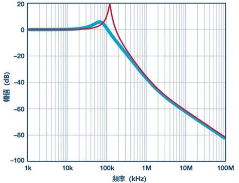
Figure 12: LC filter response (picture source: ADI)
The filter response is shown in the following figure. The red line is the original LC circuit response curve, and the blue line is the improved response curve. We see that the Q value decreases.
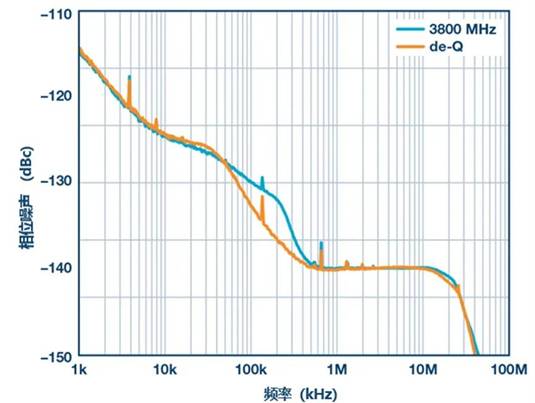
Figure 13: phase noise response (picture source: ADI)
Let‘s take a look again. For the phase noise response, the blue line is the original LC circuit response curve, and the orange line is the improved response curve. The phase noise is improved.
Summary of this paper
Noise is not only greatly different due to different power supply choices, but also may be affected by output capacitance, output voltage and load. These factors should be carefully considered, especially for sensitive supply rails.
|
Disclaimer: This article is transferred from other platforms and does not represent the views and positions of this site. If there is infringement or objection, please contact us to del
中恒科技ChipHomeTek
|


 Service mailbox
 13823783658
 ChatNow