To prevent uncontrolled operation, 4 μ The s-pause structure ensures that the system operates only in a continuous cycle 1 loop under overload or low battery input.
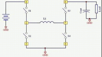
Cycle 2: Q2 and Q3 are turned on, and the energy stored in inductor L1 is transferred to the external load through Q2. At this stage, Q1 / Q4 and Q5 / Q6 are turned off. The current flow cycle is a constant value of 900ns (typical value), if CRD_ If the VCC voltage is lower than the specified value, repeat cycle 1 after this period of time.
When the output voltage reaches the specified value (1.80v, 3.0V or 5.0V), Q2 and Q3 are shut off immediately to avoid Overvoltage on the output load. At the same time, two additional NMOS Q5 and Q6 are turned on to completely discharge the current stored in the inductor and avoid ringing and voltage spikes on the system. Figure 3 shows the theoretical waveform of DC / DC converter.
When CRD_ The VCC is programmed to 0V, or when the smart card is pulled out of the socket, the active pull-down Q7 quickly discharges the output energy storage capacitor to ensure that the output voltage is less than 0.40V when the card slides on the ISO contact. Due to the low on resistance of Q7, the output voltage is less than 100 μ It drops rapidly to 400mV within s, which is far lower than the maximum value of 750 specified by EMV μ s。
Output voltage ripple, although not directly specified by iso7816-3 or EMV, plays an important role in the operation of smart card. Its peak to peak value depends on the following two main electrical parameters:
1. Total series resistance between output silicon structure and net energy storage capacitor;
2. Voltage stabilization, that is, the ability to detect the output voltage with small threshold and lag.
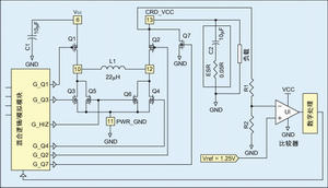
The two parameters depend on the internal welding wire connecting the chip to the outside, the pin contact connecting the series resistance of the energy storage capacitor, and the printed copper wire used to connect the pin to the load. When a large current passes through the pin, the multi welding wiring technology is widely used to reduce the series resistance to 50m (, or if a wider welding wire is used, the resistance value is lower.
The width of printed circuit board routing can be determined according to the current processing needs of a given application. In addition, the series resistance can be a problem because the external passive components involved vary greatly with different applications. The key part is the energy storage capacitor, because (for economic reasons) it is generally a low-cost type, but this will produce high voltage spikes that can hardly be completely eliminated.
Depending on the type of technology used to develop capacitors, parasitic elements may have relatively high values and produce large uncontrollable spikes. As shown in Figure 4, this equivalent series resistance (ESR) is very easy to cause such spikes because the supply current flows directly through it and brings high-voltage pulses into the output source.
Based on the experiments carried out in the characterization of ncn6001 and ncn6004a, the best scheme is to use two parallel 4.7 μ F / 10V / ceramic / X7R capacitor to realize CRD_ VCC filtering. ESR does not exceed 50m? In the whole temperature range?, Moreover, the combination of standard components provides an acceptable tolerance of - 20% to + 20%, and the cost increase is limited. Table 2 gives a general comparison of common capacitor types. Figure 5 shows the CRDs observed on the ncn6001 or ncn6004a demo board for different capacitor types for output voltage filtering_ VCC ripple. The large and fast transients observed on the above curve are very difficult to filter out because of their high energy. Clearly, aluminum capacitors are not suitable for such applications and should be avoided.
The second parameter depends on the performance of the internal comparator, voltage reference tolerance and digital processing. The voltage reference is derived from a stable bandgap circuit with a tolerance of ± 3%. On the other hand, the deviation and drift of simulation function are reduced by high-end integration technology. Detailed analysis of DC / DC operation helps to understand the impact of each element on the output voltage ripple (see figures 2 and 6).
In operation, the inductance current changes alternately between the values of IV and IP, as shown in Figure 6. When the system changes from cycle #1 inversion to cycle #2, the energy accumulated in the inductor is transmitted to the load, and the voltage of the energy storage capacitor increases with the transfer of energy to it.
Let k = R1 / (R1 + R2). When VO is greater than k * VREF, the internal comparator U1 turns over, and the output current drops to zero at time T1. Accordingly, the output capacitor contains all the energy previously stored in the inductor, and the output voltage keeps increasing above the reference value specified by parameter k * VREF. The final voltage vohp represents the amplitude of high-end ripple.
At this time, the output voltage begins to drop (because there is no more energy supplied from the inductance), and the comparator will flip when VO is less than k * VREF according to the time T2 determined by the load. The DC / DC converter continues to cycle #1 work, but the output voltage continues to drop, because it takes more time to reach the IP current value (time T3), and after the inductor is charged from zero, when it reaches the low VolP of ripple amplitude, the cycle #2 starts a new cycle. The waveform diagram of Fig. 6 describes this mechanism.
Conclusion of this paper
Under working conditions, DC / DC converter with 85% efficiency is developed and applied to smart card power supply, which can meet all complex iso7816-3 specifications. The system has sufficient robustness to prevent system latch when the load changes rapidly from zero to peak, even when the battery is at any end of the input voltage range. In addition, short-circuit current protection avoids any thermal runaway, because the trigger point of overload current will decrease with the increase of temperature. This structure has passed EMV and EMV co procedures level 1 and level 2, including EMV2000 protocol.

 Service mailbox
 13823783658
 ChatNow